Introduction
Chapter 1 - Electricity
Chapter 1.2 - The Numbers
Chapter 2 ľ Sharing and Bonding
Chapter 3 - Voltage
Chapter 3.2 ľ Voltage Static
Chapter 3.3 - Batteries
Chapter 3.4 ľ Solar - Others
Chapter 4 - Resistance
Chapter 4.2 ľ Parallel Resistance
Chapter 4.3 ľ Voltage Dividers
Chapter 5 - Semiconductor
Chapter 5.2 - PNP NPN Junctions
Chapter 6 ľ AC and Hertz
Chapter 7 - Magnetism
Chapter 7.2 - Inductors
Chapter 8 - Capacitor
Chapter 9 - IC's and OP-AMP's
Chapter 9.2 - Feedback, Unity Gain
Chapter 9.3 - Non-inverting Amplifier
Chapter 9.4 - Inverting Amplifier
Chapter 10 - 555 Timer
Chapter 10.2 - 555 Timer- Part 2
Chapter 11 - Logic
Chapter 12 - The Power Supply
Chapter 12.2 - More on Power Supplies
|
|
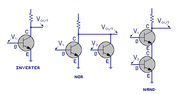
 They are either on or off. These are binary device. The same holds true with all binary
logic devices. Binary devices are generally ON or OFF, 1's or 0's, high or low, true or
false. In this section we will be using "1's" and "0's" to represent the voltage levels of
the inputs and outputs. In the NOR circuit (not or), the output moves from 1 to 0 when
V1 or V2 or both V1 and V2 move from 0 to 1. In the NAND circuit (not and) the
results are the output moving from 1 to 0 when both V1 and V2 move from 0 to 1. If
there were three or more inputs they would all have to move to get the output to move.
These are simple views and the actual circuitry is much more sophisticates.
They are either on or off. These are binary device. The same holds true with all binary
logic devices. Binary devices are generally ON or OFF, 1's or 0's, high or low, true or
false. In this section we will be using "1's" and "0's" to represent the voltage levels of
the inputs and outputs. In the NOR circuit (not or), the output moves from 1 to 0 when
V1 or V2 or both V1 and V2 move from 0 to 1. In the NAND circuit (not and) the
results are the output moving from 1 to 0 when both V1 and V2 move from 0 to 1. If
there were three or more inputs they would all have to move to get the output to move.
These are simple views and the actual circuitry is much more sophisticates.
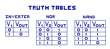
 The Bubble is a circle or large period at the beginning or end of a logic circuit.
It represents a switch in logic, both in the words used and in the voltage level. How
this works will become clearer in the next examples. The three circuits above all use
the bubble to describe the output as being opposite the input action. The Bubble is the
"NOT" or "N" part of the circuit name. Some devices with the Bubble have names like NOR and
NAND, and some devices without the Bubble are OR and AND, both
of which we will study in the next few examples.
The Bubble is a circle or large period at the beginning or end of a logic circuit.
It represents a switch in logic, both in the words used and in the voltage level. How
this works will become clearer in the next examples. The three circuits above all use
the bubble to describe the output as being opposite the input action. The Bubble is the
"NOT" or "N" part of the circuit name. Some devices with the Bubble have names like NOR and
NAND, and some devices without the Bubble are OR and AND, both
of which we will study in the next few examples.
 This graphic shows the schematic symbols for the logic functions of the NON-INVERTER,
the OR gate, the AND gate and the EXCLUSIVE OR gate. These gate devices are drawn as
two-input devices. Gates can have three, or more inputs, however their operations are
the same.
This graphic shows the schematic symbols for the logic functions of the NON-INVERTER,
the OR gate, the AND gate and the EXCLUSIVE OR gate. These gate devices are drawn as
two-input devices. Gates can have three, or more inputs, however their operations are
the same.
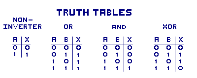 Looking at the Truth Table for the NON-INVERTER (also called BUFFER) device we see that the
input and the output are the same. When input "A" is "0", the output "X" is
"0", and when the input is 1 the output is 1. In effect a Buffer is two invertors, in series.
Looking at the Truth Table for the NON-INVERTER (also called BUFFER) device we see that the
input and the output are the same. When input "A" is "0", the output "X" is
"0", and when the input is 1 the output is 1. In effect a Buffer is two invertors, in series.
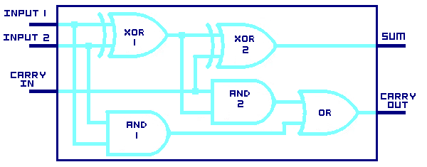
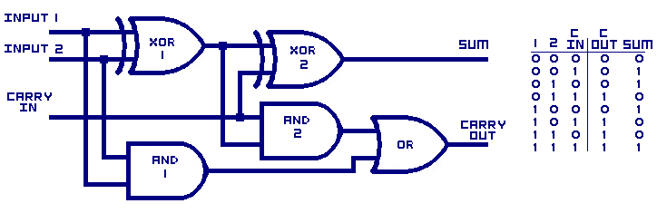 This circuit is a full Adder. Recall form Chapter One, there was
a descussion about carry, where in the 1's column carried a number
to the 10's column. In the Full Adder circuit there are three
inputs, the CARRY IN, INPUT 1 and INPUT 2 and there are two outputs,
the SUM and the CARRY OUT. Generally the CARRY IN is fed from a
previous stage and the CARRY OUT feeds another set of full adders.
This circuit is a full Adder. Recall form Chapter One, there was
a descussion about carry, where in the 1's column carried a number
to the 10's column. In the Full Adder circuit there are three
inputs, the CARRY IN, INPUT 1 and INPUT 2 and there are two outputs,
the SUM and the CARRY OUT. Generally the CARRY IN is fed from a
previous stage and the CARRY OUT feeds another set of full adders.
 Recall that during the 555 IC section the 555 was represented as a
Black Box. Here is the black box Half Adder circuit.
Because this book is not about designing
the actual components we will give our attention toward how to use
the components already on the market today.
We only care about the specification of any components
from the Black Box perspective.
Recall that during the 555 IC section the 555 was represented as a
Black Box. Here is the black box Half Adder circuit.
Because this book is not about designing
the actual components we will give our attention toward how to use
the components already on the market today.
We only care about the specification of any components
from the Black Box perspective.
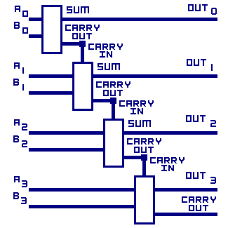 Here is a circuit putting together 4 Full Adders. This
circuit will add the two binary bits in exponent range
0 1 2 and 3 and give the correct outputs. This is a
hardware based 4-bit-set binary calculator and is much
faster then the same function build using a computer.
You can also easily expand this for additional bits.
The disadvantage of a hardware calculator is that this is all it can do.
Here is a circuit putting together 4 Full Adders. This
circuit will add the two binary bits in exponent range
0 1 2 and 3 and give the correct outputs. This is a
hardware based 4-bit-set binary calculator and is much
faster then the same function build using a computer.
You can also easily expand this for additional bits.
The disadvantage of a hardware calculator is that this is all it can do.