Schematic Objects Unity Gain Op Amp

Chapter 9.3

OP - AMP Non-Inverting


Introduction
Chapter 1 - Electricity
Chapter 1.2 - The Numbers

Chapter 2 – Sharing and Bonding

Chapter 3 - Voltage
Chapter 3.2 – Voltage Static
Chapter 3.3 - Batteries
Chapter 3.4 – Solar - Others

Chapter 4 - Resistance
Chapter 4.2 – Parallel Resistance
Chapter 4.3 – Voltage Dividers

Chapter 5 - Semiconductor
Chapter 5.2 - PNP NPN Junctions

Chapter 6 – AC and Hertz

Chapter 7 - Magnetism
Chapter 7.2 - Inductors

Chapter 8 - Capacitor

Chapter 9 - IC's and OP-AMP's
Chapter 9.2 - Feedback, Unity Gain
Chapter 9.3 - Non-inverting Amplifier
Chapter 9.4 - Inverting Amplifier

Chapter 10 - 555 Timer
Chapter 10.2 - 555 Timer- Part 2

Chapter 11 - Logic

Chapter 12 - The Power Supply
Chapter 12.2 - More on Power Supplies

Non-inverting amplifier

Op Amp - Dual-Rail Supply:

P-N Junction 
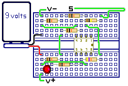
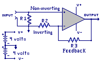
This configuration is a Non-inverting Operational Amplifier using a dual-rail supply consists of two 9 volt batteries. The supply provides +9V (one rail), with respect to the circuit common(ground) as well as a -9V (another rail).
The resistors value for R1 and R2 are 10K and the value for R3 is 100K.
Notice that there is a voltage divider circuit build around the inverter pin. One end of R2 is tied to circuit common. The other end of R2 plus the inverter pin of the Op Amp and one end of R3 make up the center of the divider. The other end of R3 is ties to the Op Amp output pin which completes the voltage divider circuit. In the schematic, one input pin of the input port to connected to the circuit common. The second input port is tied to the non-inverting. The non-inverter pin is tied through R1 to circuit common. R1 keeps the input from floating and picking up stray signals, but allows an input signal to move it around. OK, Here is how this works.


             Positive input voltage:

 1) The output is sitting at O volts due to the two input voltages
    being at 0 volts. No voltage drop is across R1, R2 or R3. The
    Op Amp is at State-2.

 2) Now by increasing the input port voltage to +0.1V, this will cause 
    non-inverter pin to signal the op amp to jump to State-3. The
    output starts to increase. The R3 starts applying that feedback
    voltage to the inverting pin until that pin also increased to
    +0.1 volts at which point the op amp switched back to stage-2.

3) Question: With both inputs +0.1V, what is the output voltage?
       Using Ohms law and the basic R2, R3 voltage divider,
       we can calculate the output voltage of the amplifier. 
       There is 0.1 volts across R2 of 10,000 ohms.
             R2 current = 0.1/10000 or 0.01mA
       There is the same 0.01mA through R3 of 100,000 Ohms.
             R3 voltage = 0.00001 X 100000 or 1V.
       Total output voltage = 0.1V(R2) + 1.0V(R3) = 1.1V 

 4) The voltage gain of the amplifier.
        The gain formula is Gain = 1 + R3/R2.
              GAIN = 1 + 100,000/10,000 or a gain of 11.
 5) Yes, the output voltage change = 11 times the input change.


             Negative input voltage:

  6) Now by decreasing the input port voltage to -0.1V, the 
    non-inverter pin will signal the op amp to jump to State-1. The
    output starts falling. The R3 starts applying that feedback
    voltage to the inverting pin until that pin also decreases to
    -0.1 volts at which point the op amp switched back to stage-2.

 7) Find the new output voltage the same way.
    There is still a voltage drop across R2 of 0.1 V,
         just in the other direction this time, so -0.1V.
    The divider current is the same as 0.01 mA in the circuit.
    Output voltage is -0.1V(R2) + -1.0V(R3) = -1.1V
    The gain is the same as 11 

Using Smooth Transitions:

P-N Junction 
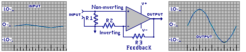
Lets reexamine this same example and replace the input voltage steps with a smooth SINE WAVE moving between -0.1V and +0.1 volts. I have graphed one cycle here. This is called a 0.2 volts peak-to-peak input signal. Because the speed of the Op Amp’s reaction to its changing inputs is sufficiently fast, the output will also be smooth with a 2.2 volt peak-to-peak output swing.


At this point in our study, we see that by providing the Op Amp with either a DC or an AC input voltage, we can, in effect, get a larger DC or AC output voltage. Thereby observing how the basic amplifier circuitry works as a voltage amplifier.

Changing Circuit Gain:

We saw in the example above that the circuit has a gain of 11. Now we will look at making changes to the feedback circuitry and thus changing the Op Amp's gain.

Changing R3:

What is the effect, if R3, the feedback resistor is changed form 100k ohms to 200k ohms. R1 and R2 remain the same and we set the input port to +0.1V
  The R2 voltage drop still needs to be 0.1v so the current through
  R2 will still be 0.01mA. 
  Voltage across R3 is E=(IxR) = 0.00001 X 200,000 or 2V.
  Total output voltage = 0.1V(R2) + 2.0V(R3) = 2.1V 

  The new gain is GAIN = 1 + 200,000/10,000 or a gain of 21.

Changing R2:

What is the effect if we now leave R3 at 200K, and change R2 to 15K. This will change both the current through the voltage divider and the gain of the amplifier.
 
  R2 voltage drop of 0.1V and 15K has a new current of 0.00667mA.
  Using that current with 200K Ohm gives 1.33V across R3
  So output voltage is 1.43 volts

  The GAIN = 1 + 200,000/15,000 or 14.3.

A couple of other thoughts.

When the input signal (sine wave) voltage is very small, placing two op amps in series, each with a gain of 11 gives a total circuit gain of 11 X 11 or 121. Three series op amps with this gain is 11 X 11 X 11 or a gain of 1331. Op amps are great for boosting very small signals but the available output voltage range is limited so additional components may be needed if a very large output voltage is needed. General purpose Op Amps are also not designed to supply large currents, so here again, if large currents are needed at the output, additional components may be needed.

Op Amp - Single Rail Supply:

P-N Junction 
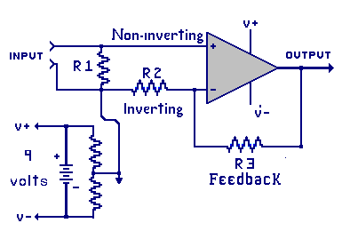
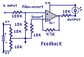
This configuration is a Non-inverting Opertional Amplifier using a single rail supply consisting of one 9 volt battery. When using a single rail supply, to replace the previous dual rail supply, there is a need to add another voltage divider circuit to provide the reference point for circuit common (ground) as supply mid-point. As drawn this circuit is using only 9 volts, which replaced the 18 volts of the last example. With half the available supply voltage the Op Amp is limited to half the output voltage swing. Note that the supply is only 9 Volts, but could be any reasonable voltage depending on the specifications of the Op Amp you choose. The higher the potential of the power supply voltage, a higher output voltage swing and a higher gain can be realized.
In simple terms, a 9 volt supply will support about a 6 v peak-to-peak output swing, while a 20 volt supply will support about a 17 v output swing.
There are some other basic Op Amp complications to address, but at this time we will not introduce additional complications to the circuitry.

Experimenting with Op Amp and LED :

Go to the work bench. Review the Resistor Color Code chart and wire up the kit as described. Perform the lab, and record your results.

In this experiment we will bring lots of our learning to this point into play. The goal of this experiment is to control the LED with the Op Amp. In this experiment we will be using a 741 Op Amp IC, powered with a single-rail power supply (9V battery). P-N Junction
Working in conjunction with the battery, there are 2 10K resistors in a voltage divider design to provide the centering of the circuit common mid way between the V+ and V- terminals of the battery. A third 10K resistor works in conjunction with a 47K resistor, forming the feedback and voltage divider circuitry for the inverting input. A forth 10K resistor working in conjunction with a 100K input resistor, forming another voltage divider as part of the non-inverting input circuitry. The fifth 10k resistor is a current limiter in series with the LED output circuitry.


 Parts List:
  1 9-volt battery
  1 Battery power clip
  5 10K ohm resistor
  1 47K Ohm resistor
  1 100K ohm resistor
  1 741 Op Amp
  1 red light emitting diode
  1 experimenters board
  wire as needed
How this works: The battery provides power to the circuit and to the voltage divider. The voltage divider is the circuit common ground mid-point of the battery voltage. This voltage is tied to the Op Amp inputs setting the output at about 4.5 volts below V+. The LED is tied to the V+ and through a 10K resistors to the Op Amp output, so there is so some current flowing through the output circuitry causing the LED to give some light.
Light Out: Taking the loose end of the S input wire, touch it to the V+, which is 4.5 volts higher then the circuit common, current flows through the non-inverting voltage divider (100K and 10K) taking that IC input to about 4.9V. This causes the op amp, with a gain of 5.7, to raise the output voltage until the feedback voltage can bring the inverting input to the same approximate 4.9V. This gain of 5.7 times the change in input voltage ( 0.4 volts) raises the output another 2.3V. With the Op. Amp output now around 6.8 V will cause the LED to be starved for current and it goes out. Recall that the LED converts current into photon energy. No current, no photons.
Light Brighter: Taking the loose end of the S input wire, touch it to the V- voltage and the reverse process happens, moving the output to about 2.3V lower then in originally was. This is about 2.2 volts output of the Op Amp. The LED is now brightly shining because of the larger current flowing through it. Lots of current, lots of photons.


« Previous Next »
Copyright 2007-2012, All Right Reserved