Introduction
Chapter 1 - Electricity
Chapter 1.2 - The Numbers
Chapter 2 – Sharing and Bonding
Chapter 3 - Voltage
Chapter 3.2 – Voltage Static
Chapter 3.3 - Batteries
Chapter 3.4 – Solar - Others
Chapter 4 - Resistance
Chapter 4.2 – Parallel Resistance
Chapter 4.3 – Voltage Dividers
Chapter 5 - Semiconductor
Chapter 5.2 - PNP NPN Junctions
Chapter 6 – AC and Hertz
Chapter 7 - Magnetism
Chapter 7.2 - Inductors
Chapter 8 - Capacitor
Chapter 9 - IC's and Amplifier
Chapter 10 - 555 Timer
Chapter 11 - Logic
Chapter 12 - Power Supply
|
|
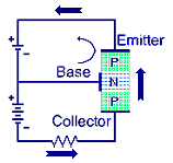
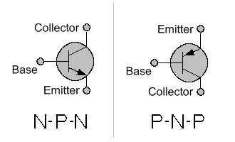 These are the schematic drawing symbols for the basic NPN and PNP transistors.
In both cases the emitter arrow is pointing toward the negative portion of the circuit
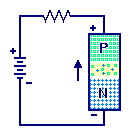
The named NPN and PNP are based on the construction materials, thus the way each
is placed into a circuit. The three legs of the transistor are called the Emitter,
Base, and Collector. The base lead is the control lead in the transistor circuit.
What that means is that it takes very
little change in base current (emitter-base current) to cause
a large change in the current flowing between the Emitter-Collector junction. The
base is an "electron" valve or gate that manages how many electrons flow through the transistor at a time.
These are the schematic drawing symbols for the basic NPN and PNP transistors.
In both cases the emitter arrow is pointing toward the negative portion of the circuit
The named NPN and PNP are based on the construction materials, thus the way each
is placed into a circuit. The three legs of the transistor are called the Emitter,
Base, and Collector. The base lead is the control lead in the transistor circuit.
What that means is that it takes very
little change in base current (emitter-base current) to cause
a large change in the current flowing between the Emitter-Collector junction. The
base is an "electron" valve or gate that manages how many electrons flow through the transistor at a time.
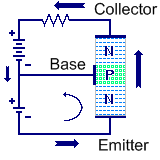
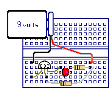
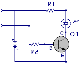 In this experiment we will be using a 2n3904 NPN transistor to
control the power for a light emitting diode (LED). By touching
the loose end of R2, the 100K resistor, to the V+ side of the 9V battery,
the transistor emitter-base junction will be activated.
This will turn on the emitter-collector junction and current will
start to flow through the transistor and LED. The LED will start
emitting photon energy.
In this experiment we will be using a 2n3904 NPN transistor to
control the power for a light emitting diode (LED). By touching
the loose end of R2, the 100K resistor, to the V+ side of the 9V battery,
the transistor emitter-base junction will be activated.
This will turn on the emitter-collector junction and current will
start to flow through the transistor and LED. The LED will start
emitting photon energy.
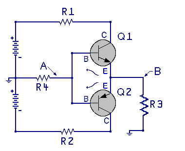
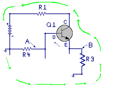 We will provide an external potential and adjust Test Point A of +2.0V.
Just at that moment, transition Q1 will see its Emitter-Base (E-B) voltage
attempt to raise.
Q1 will react, wanting to keep this junction voltage at a
proper level (around 0.7 V). To do this it will turn on and allowing current
to flow, creating a voltage drop across R3 suitable enough to restore the
Q1 junction voltage back to the desired point. Q1 will also have emitter
to collector current flowing.
At the same time Q2 will not see any need to turn on, so its E-B junction
will be off (Q2 will be acting as an insulator).
We will provide an external potential and adjust Test Point A of +2.0V.
Just at that moment, transition Q1 will see its Emitter-Base (E-B) voltage
attempt to raise.
Q1 will react, wanting to keep this junction voltage at a
proper level (around 0.7 V). To do this it will turn on and allowing current
to flow, creating a voltage drop across R3 suitable enough to restore the
Q1 junction voltage back to the desired point. Q1 will also have emitter
to collector current flowing.
At the same time Q2 will not see any need to turn on, so its E-B junction
will be off (Q2 will be acting as an insulator). 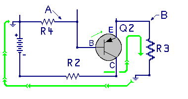 When Test Point A is set to -2.0V then Q2 will see the change in its
Emitter-Base (E-B) voltage and attempt to correct the junction voltage back to
about negative 0.7 V. In a PNP the Emitter it the most positive
voltage. At the same time Q1 will shut off and not see any need to turn on so its where
it E-B junction will be off (Q1 will be acting as an insulator). Now Q1 will
have no current flowing and Q2 will have emitter to collector current flowing. In the Q2
circuit the ground or 0 voltage level is the highest voltage in the circuit
and the battery is providing a -5 volt supply to the circuit.
When Test Point A is set to -2.0V then Q2 will see the change in its
Emitter-Base (E-B) voltage and attempt to correct the junction voltage back to
about negative 0.7 V. In a PNP the Emitter it the most positive
voltage. At the same time Q1 will shut off and not see any need to turn on so its where
it E-B junction will be off (Q1 will be acting as an insulator). Now Q1 will
have no current flowing and Q2 will have emitter to collector current flowing. In the Q2
circuit the ground or 0 voltage level is the highest voltage in the circuit
and the battery is providing a -5 volt supply to the circuit.