Schematic Objects Unity Gain Op Amp

Chapter 9.4

OP AMP - Inverting


Introduction
Chapter 1 - Electricity
Chapter 1.2 - The Numbers

Chapter 2 – Sharing and Bonding

Chapter 3 - Voltage
Chapter 3.2 – Voltage Static
Chapter 3.3 - Batteries
Chapter 3.4 – Solar - Others

Chapter 4 - Resistance
Chapter 4.2 – Parallel Resistance
Chapter 4.3 – Voltage Dividers

Chapter 5 - Semiconductor
Chapter 5.2 - PNP NPN Junctions

Chapter 6 – AC and Hertz

Chapter 7 - Magnetism
Chapter 7.2 - Inductors

Chapter 8 - Capacitor

Chapter 9 - IC's and OP-AMP's
Chapter 9.2 - Feedback, Unity Gain
Chapter 9.3 - Non-inverting Amplifier
Chapter 9.4 - Inverting Amplifier

Chapter 10 - 555 Timer
Chapter 10.2 - 555 Timer- Part 2

Chapter 11 - Logic

Chapter 12 - The Power Supply
Chapter 12.2 - More on Power Supplies

Inverting Amplifier

Op Amp - Dual Rail Supply:

P-N Junction 
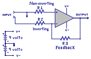
This configuration is a Inverting Operational Amplifier using a dual-rail supply consists of two 9 volt batteries. The supply provides +9V (one rail), with respect to the circuit common(ground) as well as -9V (another rail).
The resistors value for R1 and R2 are 10K and the value for R3 is 100K.
Notice that one input port, feeds into R2. The other end of R2 and R3 form a voltage divider circuit around the inverting input pin, with R3 being the feedback circuit. The IC's inverting voltage is a sum of the sources of R2 and R3. In the schematic drawing, the other input port is connected to the circuit common.
The non-inverter pin is tied through R1 to circuit common. R1 keeps the input from floating and picking up stray signals. In this amplifier the input changes will all take place on the inverting input circuitry. OK, Here is how this works.


             Positive input voltage:

 1) The output is sitting at O volts due to the two input voltages being
    at 0 volts. No voltage drop is across R1, R2 or R3. The Op Amp is at
    State-2.
  
 2) When a +0.1 V is applied to the inverting signal input terminal, current
    will start to flow through R2, which will increase the inverting pin
    voltage above the non-inverting pin.  The Op Amp moves to state-1 and
    the output voltage starts moving down toward the V- voltage. This
    continues until R3 can pull the voltage applied through the voltage
    divider to the inverting pin to the same potential as the non-inverting
    pin.  
   
 3) Question: With the input port voltage at +0.1v and both IC inputs
       back to 0.0V, what is the output voltage?
       Using Ohms law and the basic R2, R3 voltage divider,
       we can calculate the output voltage of the amplifier. 
       There is 0.1 volts across R2 of 10,000 ohms.
             R2 current = 0.1/10000 or 0.01mA
       There is the same 0.01mA through R3 of 100,000 Ohms.
             R3 voltage = 0.00001 X 100000 or 1V.
    Output voltage is - 1.0 volts.
    SO: It takes 1.0V output in the negative direction to
        offset the 0.1V input to keep the inverting pin at 0.0V
 
 4) The voltage gain of this amplifier.
        The GAIN equals R3/R2 or 100K/10K or a GAIN of 10


             Negative input voltage:

 5) Now by decreasing the input port voltage to -0.1V, the 
    inverter pin will signal the op amp to jump to State-3. The
    output starts increasing. The R3 starts applying that feedback
    voltage to the inverting pin until that pin returns back to 
    0.0 volts at which point the op amp switched back to stage-2.

 6) Find the new output voltage the same way.
    There is still a voltage drop across R2 of 0.1 V,
         just in the other direction this time, so -0.1V.
    The divider current is the same as 0.01 mA in the circuit.
    Output voltage is +1.0V
    The gain is the same at 10            

There are a number of different operational amplifiers on the market today. Some models like the CA3033, are no longer available and new IC's show up on the market from time to time. One of the most common over the years is the 741. There are additional letters and numbers as part of the actual part number to designate manufacturers, temperature ranges and alike. Op Amps come in many different pin configurations and specifications. Here is a short list of some common IC's.

 Id    = general part identification
 Slew  = slew rate is output voltage change per microsecond.
 Volts = power supply voltage range
 Tmp   = operating temperature limits in degrees C
 Cost  = general cost range (reference not actual cost) 

 
 Single op amp in a package
  ID   Slew     Volts         Tmp          Cost
 3140  9.0V   4V to 36V   -55 to 125 C   2.50 dollars
  201  0.5V   5V to 22V   -25 to  85 C   0.50 dollars
 2904  0.1V   3V to 26V   -40 to 125 C   1.50 dollars
  747  0.5V   10V to 36V    0 to  70 C   0.50 dollars
 OP07  0.3V   3V to 18V     0 to  70 C   0.50 dollars

 Dual and Quad Op Amps
  ID   Slew    Volts          Tmp         Cost
 158   0.6V   3V to 30 V  -55 to 125 C 	 2.50 dollars
 258   0.6V   3V to 30 V  -25 to  85 C 	 0.50 dollars
 358   0.6V   3V to 30 V    0 to  70 C   0.50 dollars				
 324   0.5V   4V to 32V     0 to 70 C    0.50 dollars


  You can see from these sample charts that if you want an IC that is very
  fast, and can work outside both summer and winter the 3140 is the fastest
  one here with a wide temperature range, and a higher reference cost.


« Previous Next Chapter »
Copyright 2007-2012, All Right Reserved