Schematic Objects 555 IC

Chapter 10.1

Good Times With Timers


Introduction
Chapter 1 - Electricity
Chapter 1.2 - The Numbers

Chapter 2 – Sharing and Bonding

Chapter 3 - Voltage
Chapter 3.2 – Voltage Static
Chapter 3.3 - Batteries
Chapter 3.4 – Solar - Others

Chapter 4 - Resistance
Chapter 4.2 – Parallel Resistance
Chapter 4.3 – Voltage Dividers

Chapter 5 - Semiconductor
Chapter 5.2 - PNP NPN Junctions

Chapter 6 – AC and Hertz

Chapter 7 - Magnetism
Chapter 7.2 - Inductors

Chapter 8 - Capacitor

Chapter 9 - IC's and OP-AMP's
Chapter 9.2 - Feedback, Unity Gain
Chapter 9.3 - Non-inverting Amplifier
Chapter 9.4 - Inverting Amplifier

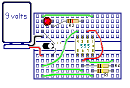
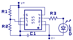
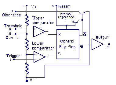
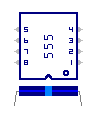
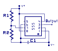
Chapter 10 - 555 Timer
Chapter 10.2 - 555 Timer- Part 2

Chapter 11 - Logic

Chapter 12 - The Power Supply
Chapter 12.2 - More on Power Supplies

555 Timer Oscillator

In this chapter we are looking at the 555 IC used as a timer oscillator. This is a very versatile and interesting integrated circuit that has been used in many university courses, and in the electronic industry. There are times when a oscillator or tone generator of some type is needed. The lower priced, lower precision solution of using the 555 or the 7555 chip will work just fine. There is an added benefit of saving several hundred dollars or more over a commercial generator. The 7555 IC, using advanced technology, consumes less power then the 555, thus commanding a higher price tag.

At the foundation of the 555, we start with input circuitry which has two Op Amps working as comparators and called the lower and upper comparator. They feed into a toggle circuit called a Flip-Flop. The output is a unity amplifier, Additionally the 555 has a few other components inside. P-N Junction
Pin layout for the 555 chip is an 8-pin dual inline pin (8-dip) arrangement. The case is marked with either a small circle, or a u-shaped notch at one end of the top surface of the body. Moving counter-clockwise (anti-clockwise) from that marker, the pins are numbered 1, 2, 3, and 4 on one side of the body, and continue on the other side as 5, 6, 7, and 8.

555 IC This illustration shows the basic 555 circuitry.
There are three internal resistors, acting as a voltage divider between V+ and V-. The divider sets the input voltage on the non-inverting lower comparator to 1/3 supply voltage and the inverting input voltage (the upper comparator) to 2/3 supply voltage.
In previous sections and labs we learned how the voltage divider and the Op Amps work. When an Op Amp is a comparator there is no feedback. This means that the output is either high or it is low (review state-1 and state-3 in eariler sections). Now we will take a brief look at the Flip-Flop component in the 555 circuitry.

Flip-Flop Truth Table

 A truth table tells how the IC works in table form. This short hand
 tool makes quick work of learning how any Black Box circuit works.
 Here is how the Flip-Flop circuit Truth Table works.

 In a truth-table  0 represents no voltage, off, or false,
              and  1 represents high voltage, on, or true.

 NOTE: In a truth-table the IC inputs determine the IC outputs.
       You may have some control over inputs but the as a black
       box the IC controls its outputs based on its inputs.

            Truth Table for the Flip-Flop inside the 555   
      R     S     Not-Q     Q
      0     1      0        1   
      1     0      1        0

 There are two input R, and S and two outputs Q and not-Q.
 In this table when        R is  0  and S is  1
   the outputs are     Not-Q is  0  and Q is  1, as indicated.

 In the other state when   R is  1  and S is  0 
    then               Not-Q is  1  and Q is  0.

 The other two options where R and S are either both 0 or both 1
 there is no change to the outputs Q and Not-Q.

The 555 Pin-out (description)

 Pin 1: V-, circuit ground or common
 Pin 2: Trigger Input
 Pin 3: Output
 Pin 4: Reset, during a falling voltage level
        the 555 output is reset to low voltage
 Pin 5: Control input
 Pin 6: Threshold
 Pin 7: Discharge
 Pin 8: V+

The 555 in Astable Multivborator Configuration

This general oscillator with the big name, has a simple meaning. The astable portion means that there is “no stable” output. The multivibrator portion means that there are output-states. 555RexOsc
In other words the output changes all the time. In this circuit, by wiring two resistors R1 and R2 and a capacitor C1 of proper values, to the inputs as shown in the illustration, the 555 operates as an oscillator.

Theory of Operation:

At time-period 0, with power applied to the circuit, the lower comparator output is at voltage 1. The upper comparator output is at voltage 0. The output on the 555 IC is at voltage 1. R1 and R2 start charging capacitor C1.
At some time-period, 1, the capacitor voltage level at 555 IC pin 2, which is the lower comparator inverting input, becomes higher then the 1/3 supply voltage fed to the non-inverting input. The lower comparator output now switches low, which supplies a 0 voltage to the S flip-flop input.
The capacitor continues to charge and at time-period 2, the upper comparator at pin 6, being an non-inverting input becomes greater then 2/3 of the supply voltage, causing this comparator output to go high, which supplies a 1 voltage to the R input of the flip-flop.
At this moment the flip-flop will switch output states. Output Q goes from a 1 to a 0. This drives the unity amplifier to follow Q, to provide a 0 at the output pin number 3 of the IC. at the same moment in time, Not-Q is switched high, which turns on the discharge transistor. Now C1 starts to discharge through R2 and the internal transistor.
At time-period 3, the 555 IC pin 6 upper comparator voltage drops below 2/3 supply voltage, which caused the upper comparator to supply a 0 to the R input of the Flip-flop.
The C1 capacitor voltage continues to discharge until time-period 4, where 555 IC pin 2 drops below the 1/3 supply voltage on the lower comparator. At this moment the lower comparator output switches to a 1 causing the flip-flop to switch output states with Q now at 1 and not-Q now at 0. The output on the IC pin 3 is now high again. The discharge transistor is shut off, and the cycle starts over at time 0.

This circuit has just passed through one timing cycle and it starts over again with the capacitor starting to charge through R1 and R2. Now that we know the cycle, how fast does all this happen?
This is where we apply those RC time constants we studies earlier in the book. The full RC time cycle triggering the flip-flop circuitry and changing the output stage is a set of two half cycles. The first half-cycle is for the charging of C1 through R1 and R2. The second half-cycle is the discharging of C1 through R2.

 First Half-cycle t1 = 0.693 x (R1 + R2) x C1
   During this cycle the output is HIGH
 Second Half-Cycle t2 = 0.693 x R2 x C1
   During this cycle the output is LOW.
  

Astable Multivibrator class circuits can be implemented using IC including this 555 Timer or the 7555 IC timer, an array of different logic gates, transistorized circuits, and older technologies include vacuum tube based circuitry and relay based devices.

Experiment with the 555 Timer IC and an LED:

555 and led Go to the work bench. Review the Resistor Color Code chart and wire up the kit as described. Perform the lab, and record your results.


555RexOsc
Parts List:
  1 9-volt battery
  1 Battery power clip
  1 555 IC - U1
  1 10 mmf capacitor - C1
  1 1 k ohm resistor - R3
       (brown, black, red)
  2 100 k ohm resistor - R1, R2
       (brown, black, yellow)
  1 red light emitting diode
  1 experimenters board
  Miscellaneous:
    hookup wire
555 LED


NOTES: The flat side of the LED is toward the V- side of the circuit. The minus side of the C1 capacitor is toward the V- side of the circuit.


« Previous Next Chapter »
Copyright 2007-2012, All Right Reserved